
The Semiconductor Fab Lifecycle: From Sand to Silicon
Semiconductor fabrication plants, commonly known as "fabs", are the most complex and expensive manufacturing facilities in human history. With modern megaprojects costing anywhere from $10 Billion to $30 Billion, building a fab requires monumental capital, precise engineering, and years of execution.
1. Planning & Site Selection (Planned Fabs)
Before a shovel even touches the dirt, companies like TSMC, Intel, and Samsung spend years scouting locations. A viable site requires:
- Massive Power: A single advanced fab consumes up to 100 megawatts of electricity per hour, enough to power a small city.
- Abundant Water: Making chips requires millions of gallons of ultra-pure water daily to rinse silicon wafers between manufacturing steps.
- Geopolitical Support: Recent expansions are heavily influenced by government incentives, such as the U.S. CHIPS and Science Act or the European Chips Act, pushing companies to build in Ohio, Arizona, and Germany.
2. Construction: Building the Cleanroom (Fabs Under Construction)
Constructing a fab isn't like building a standard factory. The heart of the plant is the Cleanroom, which must be up to 10,000 times cleaner than an operating room. The construction process involves pouring massive concrete foundations designed to isolate the building from micro-vibrations (even vibrations from a nearby highway can ruin nanoscale chip patterns).
Beneath the cleanroom lies the "Subfab," a multi-story basement filled with the pumps, chillers, and chemical delivery systems required to safely handle the highly toxic gases and liquids used in semiconductor manufacturing.
3. Equipment Move-In (MEP)
Once the shell is built, the most critical (and expensive) phase begins: moving in the tools. A modern logic fab relies on Extreme Ultraviolet (EUV) Lithography machines built exclusively by the Dutch company ASML.
A single EUV machine costs over $150 million, weighs 180 tons, and requires three Boeing 747s just to ship. Installing and calibrating a fleet of these machines takes months of meticulous work by specialized engineers.
4. Process Ramping & Yield
After the machines are powered on, the fab enters the "ramp" phase. Manufacturers don't instantly produce perfect chips. They run thousands of test wafers to tune their processes.
The goal is to maximize the Yield, the percentage of perfectly functioning chips on a single silicon wafer. At advanced nodes like 3nm and 2nm, achieving a profitable yield rate can take over a year of continuous refinement.
5. High-Volume Manufacturing (Active Fabs)
Once high yield is achieved, the fab enters High-Volume Manufacturing (HVM). The plant will run 24 hours a day, 7 days a week, 365 days a year. Fabs are measured by their capacity, often stated in Wafers per Month (WPM). A modern megafab might process 50,000 to 100,000 silicon wafers every month, churning out millions of processors for smartphones, cars, and data centers around the world.
Semiconductor playlist
Semiconductor Industry Glossary
- Foundry
- A company that manufactures chips designed by other companies (e.g., TSMC, GlobalFoundries). They do not design their own products.
- IDM (Integrated Device Manufacturer)
- A company that both designs and manufactures its own semiconductor chips (e.g., Intel, Samsung, Texas Instruments).
- Fabless
- A company that designs chips but outsources the physical manufacturing to a foundry (e.g., NVIDIA, AMD, Qualcomm, Apple).
- OSAT (Outsourced Semiconductor Assembly and Test)
- Companies that package and test the silicon dies after they are manufactured by a foundry, turning them into the final chips you see on a circuit board.
- Wafer
- A thin slice of highly purified silicon used as the base material for microchips. Modern advanced fabs process 300mm (12-inch) diameter wafers.
- Node (e.g., 3nm, 5nm)
- A marketing term used to describe the generational advancement of semiconductor manufacturing. Originally indicating the physical size of transistor gates, it now simply signifies a new generation of increased density and efficiency.
- EUV (Extreme Ultraviolet Lithography)
- The state-of-the-art technology used to print the most advanced microchips (7nm and below). ASML is the sole manufacturer of these machines.
- Tapeout
- The final phase of the chip design process where the completed blueprint is sent to the foundry to begin physical manufacturing.
- Yield
- The percentage of manufactured chips on a wafer that function correctly without defects. High yield is crucial for profitability.
Recommended Reading & Resources
To dive deeper into the history, geopolitics, and engineering behind global semiconductor manufacturing, we highly recommend the following books:

Chip War
A gripping geopolitical history of the struggle for microchip supremacy, detailing how this tiny technology shapes the global balance of power.
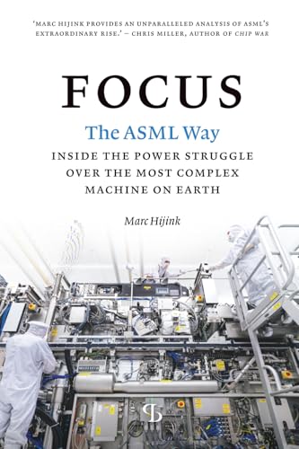
Focus: The ASML Way
The inside story of the Dutch tech giant that manufactures the world's most critical EUV lithography machines, enabling the smallest chip nodes.

The Idea Factory
A deep dive into Bell Labs, the cradle of modern innovation where the transistor, information theory, and silicon solar cells were invented.

The Nvidia Way
A definitive, inside look at Nvidia’s meteoric rise to become the world’s most valuable chip company, driven by Jensen Huang’s relentless vision for AI and GPU computing.

Microchip Fabrication
A comprehensive, industry-standard guide to every phase of semiconductor processing, covering everything from raw materials to wafer testing and packaging.

Physics of Semiconductor Devices
The classic, foundational reference text detailing the physics and operational principles behind contemporary microelectronic and optoelectronic devices.

Semiconductor Physics and Devices
An engaging and rigorous textbook introducing solid-state physics, quantum mechanics, and the basic principles of semiconductor devices.
Ready to explore? View our Interactive Global Fab Map.